
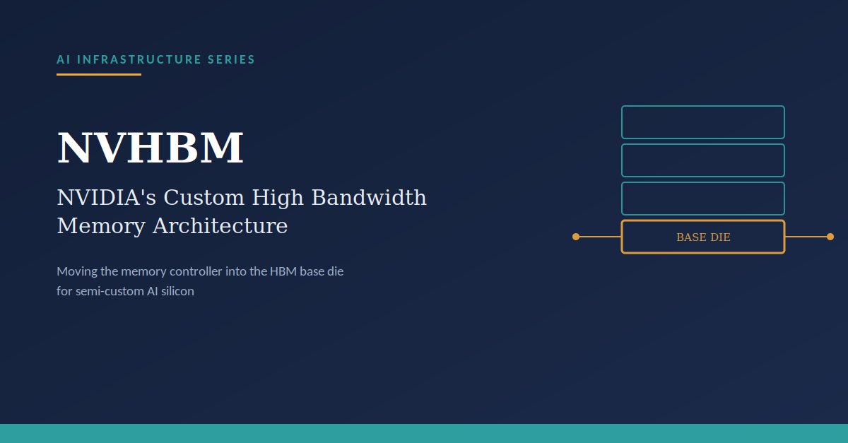
NVHBM: NVIDIA's Custom High Bandwidth Memory Architecture for Semi-Custom AI Silicon
Recently, NVIDIA introduced a new architecture, called NVHBM, which pulls the memory controller out of the XPU chip and puts it inside the HBM stack's own base die. Amazon's Annapurna Labs is already on board for Trainium4.

HBM4: JEDEC's Next-Generation High Bandwidth Memory Standard
HBM4 is JEDEC's answer, standardized as JESD270-4 in April 2025 with input from AMD, Nvidia, Google, SK hynix, Samsung, Micron, and other major players. It roughly doubles per-stack bandwidth over HBM3, and it does something more interesting than just “go faster”: it fundamentally changes who gets to design part of the memory stack.

ZAM: Intel and SoftBank's Bold Bet on the Memory Front
ZAM is a stacked DRAM architecture, conceptually similar to HBM but with a fundamentally different approach to how the layers are connected and how heat escapes.

CXL is Alive and Kicking!
In this article, I will talk about some of the recent CXL implementations, most of them geared to serve the insatiable appetite of AI compute infrastructure.
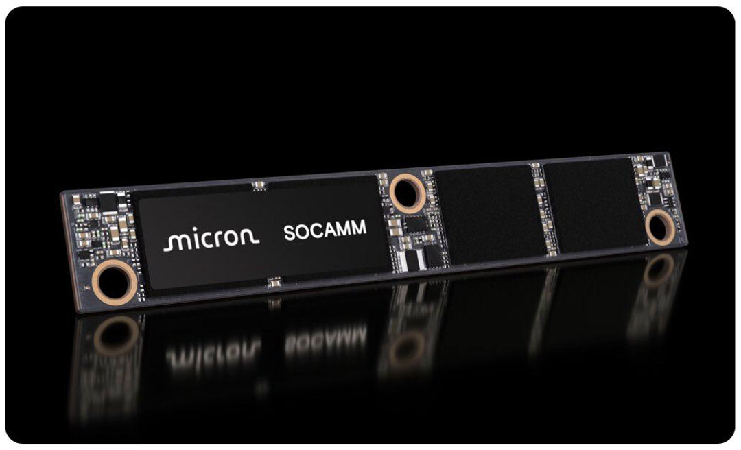
SOCAMM: Yet Another Framework on the Memory Horizon
The SOCAMM memory leverages the LPDDR5X memory, which, as the name states, is a Low Power memory. However, LPDDR is a soldered-down memory leaving no room for repair and field-replaceability; thereby increasing the total cost of ownership. (TCO) SOCAMM is a screws-secured, socketed memory
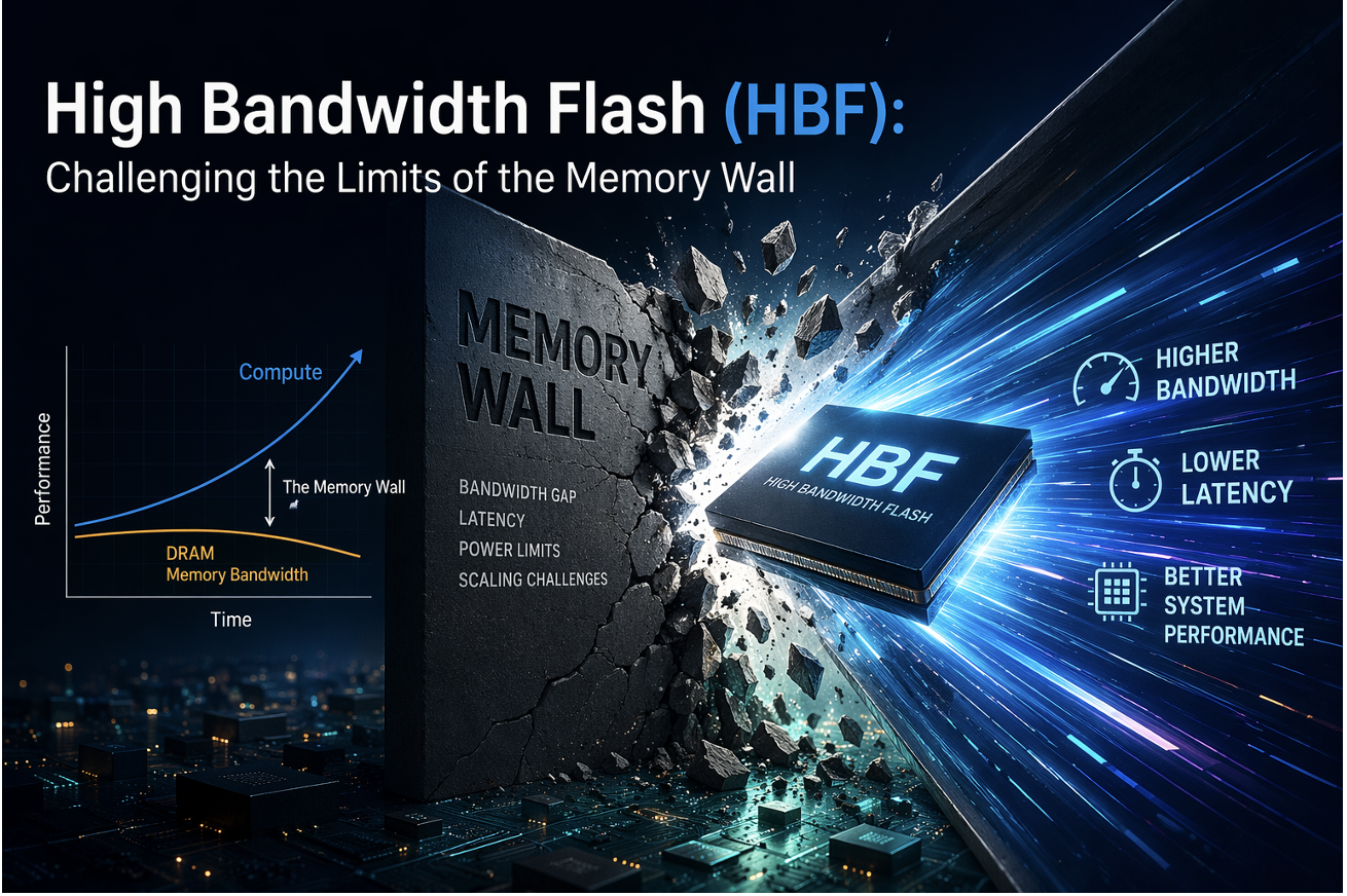
Crumbling the Memory Wall with High Bandwidth Flash (HBF)
Enters High Bandwidth Flash or HBF, which aims to serve as an intermediary layer between HBM and the slower NVMe SSDs. The base architectural concept remains similar to HBM.Enters High Bandwidth Flash or HBF, which aims to serve as an intermediary layer between HBM and the slower NVMe SSDs. The base architectural concept remains similar to HBM.