
HBM4: JEDEC's Next-Generation High Bandwidth Memory Standard
Last time, I wrote about High Bandwidth Flash (HBF), an attempt to borrow HBM's packaging tricks and marry them to NAND Flash so that we get a cheaper, denser “mid-tier” memory sitting between HBM and SSDs. Before that, I covered CXL and SOCAMM. If you have been following this series, you already know the running theme: the memory wall isn't going away, and the industry keeps inventing new ways to climb over it, tunnel under it, or, in HBM4's case, redesign the wall itself.
This time, I am going back to the memory that started the whole AI hardware conversation: HBM. Specifically, its sixth generation, HBM4 (after HBM1, HBM2, HBM2E, HBM3, and HBM3E), which is no longer a roadmap slide; it is shipping.
Why HBM4, and Why Now
Every GPU generation (after a point of time in history) has been memory-starved in one way or another. Trillion-parameter models, agentic workloads juggling long-lived KV caches, and inference workloads that never really “finish” reading from memory have all pushed bandwidth and capacity demands higher than DRAM scaling alone can satisfy. HBM3E, the memory riding on today's Hopper and Blackwell-class GPUs, is a capable workhorse: it comfortably delivers over a terabyte per second per stack and has powered the current generation of AI training and inference. But it is also, by 2026 standards, starting to show its age.
HBM4 is JEDEC's answer, standardized as JESD270-4 in April 2025 with input from AMD, Nvidia, Google, SK hynix, Samsung, Micron, and other major players. It roughly doubles per-stack bandwidth over HBM3, and it does something more interesting than just “go faster”: it fundamentally changes who gets to design part of the memory stack.
What HBM4 Actually Changes
At the JEDEC-standard level, the headline numbers are straightforward. HBM4 widens the interface from 1,024 bits to 2,048 bits and doubles the number of independent channels per stack from 16 to 32, each split into two pseudo-channels. That wider, more parallel interface is how HBM4 reaches upward of 2 TB/s per stack at the standard's baseline pin speeds, with vendors already sampling well past that on custom silicon. Capacity per stack scales up to 64 GB, which starts to make “nearly 400 GB of HBM on a single GPU package” a realistic sentence to write, rather than a marketing one.
Power efficiency gets attention too. JESD270-4 supports multiple vendor-specific voltage levels for signaling and core power, and the standard's Directed Refresh Management feature is aimed at squeezing more efficiency out of refresh operations, a small-sounding detail that matters a great deal when you are running thousands of these stacks per rack.
But the real story of HBM4, the one that will matter more than any single bandwidth number, is what's happening to the base die.
The Base Die Becomes a Chiplet
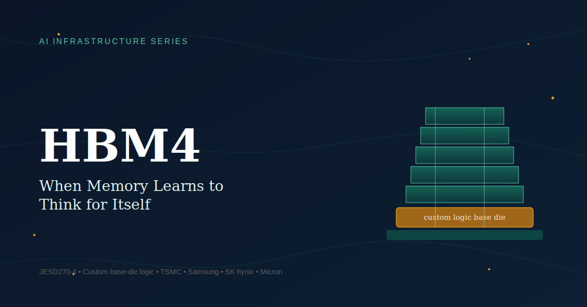
In every HBM generation up to HBM3E, the base die, the logic layer sitting underneath the stacked DRAM dies, acting as the interface between the stack and the host processor, was manufactured on essentially the same DRAM process as the memory dies above it. It was, functionally, a signal pass-through: simple, cheap, and identical for every customer.
HBM4 breaks that pattern. The base die is now built on an advanced logic process, separate from the DRAM core dies, which turns it into something closer to a customizable chiplet than a memory component. SK hynix has partnered with TSMC to fabricate its HBM4 base die on a 12nm process for Nvidia's current generation, while Samsung has gone the vertically integrated route, building its own base die in-house on a 4nm process and handling the 3D packaging under one roof. Micron, meanwhile, has handed its HBM4E base die fabrication to TSMC as well, explicitly to open the door to customer-specific logic.
Nvidia itself is reportedly working on designing its own logic dies for a future HBM generation, perhaps, to claw back some architectural control from the memory makers.
Whether you think of HBM4 as “faster HBM” or as “the moment memory became semi-configurable silicon,” both are true. But the second framing is the one worth remembering.
What This Looks Like in Silicon, Today
Samsung became the first company to announce global mass production of HBM4 commercially, in February 2026, using a 4nm logic base die paired with 12-high stacking, and is reporting data rates around 11.7 Gbps and bandwidth near 3.3 TB/s per stack, comfortably ahead of the JEDEC baseline. Samsung has also demonstrated hybrid bonding, fusing copper pads directly together without traditional micro-bumps, which reduces stack height and improves heat dissipation, and is already talking about a 16-high stack pushing per-stack capacity to 48 GB.
SK hynix, which entered HBM4 with a commanding share of the HBM3E market, has taken the more distributed route: DRAM core dies from its own fabs, paired with a TSMC-fabricated logic base die, initially on a 12nm node and reportedly moving toward 3nm for HBM4E. SK hynix's HBM4 has also been reported to exceed the JEDEC baseline meaningfully on data rate.
On the platform side, Nvidia's Vera Rubin architecture is the headline HBM4 consumer: eight HBM4 stacks per GPU package, a starting capacity in the 288 GB range, and theoretical aggregate memory bandwidth as high as 22 TB/s. AMD's MI400-class accelerators are the other big HBM4-era platforms of 2026. A successor tier, HBM4E, is already on manufacturers' roadmaps for 2027, targeting per-stack bandwidth in the 3.6 - 4 TB/s range and even deeper customization of the base die.
Ecosystem and Adoption
The ecosystem here is, unsurprisingly, the same trio that has always anchored HBM: SK hynix, Samsung, and Micron, all racing to ship HBM4 and its HBM4E follow-on. What's new is TSMC's role. Historically a bystander to HBM, which memory makers built and packaged largely in-house, TSMC is now fabricating custom logic base dies for SK hynix and Micron, and expanding its CoWoS-L advanced packaging line specifically to handle 12-and-beyond-high HBM4 stacks. That is a meaningful shift in who has leverage in the HBM supply chain, and it is part of why Nvidia is reportedly interested in designing its own base-die logic for a future generation; control over the base die is quickly becoming as strategically important as control over the GPU itself.
On the consumption side, Nvidia, AMD, and Google are the anchor customers, with Microsoft and Broadcom also named as recipients of customized HBM4E base dies from SK hynix. This is a narrower ecosystem than, say, CXL's sprawling list of controller and switch vendors, which is a fair reflection of how concentrated the HBM supply chain has always been.
Honest Caveats
This series has always tried to name the rough edges, and HBM4 has a few worth sitting with.
Yield and thermal risk are real, not theoretical. Moving from 12-high to 16-high stacks means DRAM dies thinned to around 30 microns, and hybrid bonding at that scale demands sub-micron alignment precision across every layer. Samsung's own redesigned DRAM core die, used in its HBM4, reportedly ran lower yields during parts of its development; improving over time, but underscoring how unforgiving this process still is.
Customization cuts both ways. A base die tailored to Nvidia's Rubin architecture is not necessarily one that serves AMD or a hyperscaler's custom accelerator equally well. The more HBM4 becomes semi-custom silicon, the more the memory supply chain starts to resemble the fragmented, allocation-driven world of leading-edge logic rather than the comparatively fungible commodity memory of the past.
HBM4E is not yet a unified standard. Samsung, SK hynix, and Micron are each pursuing their own specifications for pin speed, process node, and packaging, which means “HBM4E” today is closer to a marketing umbrella than a single interoperable spec.
Nobody seriously claims HBM4 solves the memory wall outright. It buys more bandwidth and more capacity per package, and it opens a new axis of customization, but the fundamental tension between compute growth and memory growth is still there. HBM4 is a strong next step, not a finish line.
Outlook
If HBM3E was about proving that stacked memory could keep pace with AI accelerator demand, HBM4 is about proving that memory itself can become a customizable part of the compute stack, not just a commodity bolted onto it. The base-die shift toward advanced logic nodes, and the growing involvement of a pure-play foundry like TSMC in what used to be a memory-maker's internal process, both point toward a future where “who designs your memory” becomes as consequential a decision as “who designs your GPU.”
Expect 16-high stacks and hybrid bonding to become mainstream through the back half of 2026, HBM4E specifications to firm up through 2027, and if the disaggregation conversations already circulating in the industry go anywhere, a future where HBM4-class stacks are pooled and shared across compute nodes the way this series has already described for CXL-attached DRAM. The memory hierarchy keeps getting more interesting, not less.
As always, if I've missed a development, an implementation, or a company doing something worth covering here, tell me in the comments — I'll keep adding to the story as it unfolds.
References
https://www.allaboutcircuits.com/news/jedec-officially-releases-hbm4-memory-standard/
https://blogs.sw.siemens.com/semiconductor-packaging/2026/04/24/hbm3e-hbm4-ic-design-guide/
https://www.kynix.com/Blog/hbm3e-vs-hbm4-2026-specs-performance--supply-guide.html
https://www.tomshardware.com/micron-hands-tsmc-the-keys-to-hbm4e
https://www.oscoo.com/news/hbm4-the-memory-revolution-in-the-age-of-ai-computing/
https://www.eetimes.com/the-state-of-hbm4-chronicled-at-ces-2026/
https://newsletter.semianalysis.com/p/isscc-2026-nvidia-and-broadcom-cpo
https://www.digitimes.com/news/a20250724PD223/samsung-hbm4-production-2026-sk-hynix.html
https://www.techinsights.com/outlook-reports-2026/advanced-packaging-outlook-report
https://wccftech.com/jedec-approves-sphbm4-to-break-hbm-costs-retain-hbm4-speeds-standard-packages/
