
Semicon 2.0: India's Next Phase in the Global Chip Race
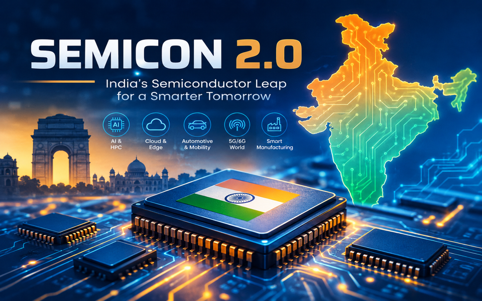
On July 15, 2026, the Union Cabinet approved Semicon 2.0, the second phase of India's semiconductor policy, with a fiscal outlay of ₹1,27,500 crore (roughly $13.3 billion). While the numbers look good, I believe it’d be good to look at what Semicon 2.0 actually proposes, how it builds on its predecessor, and where there are gaps, still.
This article isn't part of my usual AI infrastructure series on interconnects and memory. Semicon 2.0 is a policy and industrial-strategy story, not a protocol or standard, so I'm treating it as a standalone read.
From Semicon 1.0 to Semicon 2.0
India Semiconductor Mission 1.0 (Semicon 1.0) launched with an outlay of ₹76,000 crore for building out the country's semiconductor and display manufacturing ecosystem. Of that, roughly ₹64,000 crore was earmarked for chip fabs, ₹10,000 crore for a semiconductor lab, and ₹1,000 crore for a design-linked incentive scheme.
According to the government's own account, 1.0 delivered real, if early-stage, traction. Twelve manufacturing units have been approved with a cumulative investment of over ₹1.64 lakh crore — one silicon fab, one silicon carbide fab, an integrated gallium nitride micro-LED display fab, and nine packaging units. Three companies, Micron, Kaynes, and CG Semi, have started commercial production, with one more expected to follow in 2026. On the design side, 24 semiconductor design projects have been approved for financial support, and 105 startups and MSMEs now have access to industry-standard EDA tools, working on everything from satellite communication and drones to IoT devices and AI systems.
Independent trackers of the mission, however, put the number of approved 1.0 manufacturing projects at 10 rather than 12, and there is no single published evaluation report reconciling the two counts. I have gone with the government's own July 2026 figure as the primary number.
What Semicon 2.0 Actually Proposes
Semicon 2.0 is explicitly framed by the government as a shift from a fab-centric scheme to a full ecosystem play. Rather than concentrating incentives on fabrication alone, the ₹1,27,500 crore outlay is built around six pillars:
Design: deepening India's chip and IP design base beyond the 105 startups already working with EDA tools, with an explicit goal of making India a chip-design-IP hub rather than only a downstream assembler.
Machines and materials: incentivizing the manufacturing and R&D of the equipment, chemicals, and gases that fabs actually consume, since none of that supply chain exists domestically today.
More fabs: attracting additional silicon, compound-semiconductor, discrete-component, and display fabs, building on the first commercial silicon fab, which remains scheduled for commissioning in 2028.
ATMP/OSAT: extending assembly, test, marking, and packaging capacity, with a push toward more advanced packaging technologies rather than only mature-node packaging.
Research & development: moving beyond the 28nm–110nm node range that 1.0 largely operated in, toward more advanced nodes in partnership with R&D centres in India and abroad.
Talent development: deepening training across the 315 universities and roughly 68,000 students already exposed to chip-design tooling, and extending it into fab-construction and clean-room skills.
The government's stated rationale is straightforward: fabs alone do not make a semiconductor ecosystem. Without domestic capability in equipment, specialty chemicals, and advanced packaging, India would keep building fabs on top of an imported supply chain, which is precisely the gap Semicon 2.0's second and fourth pillars are meant to address.
How India's Bet Compares Globally
It is tempting to line Semicon 2.0's $13.3 billion up against the other national chip programs making headlines, but the accounting bases differ enough that a direct dollar-for-dollar comparison is misleading. Still, the rough shape is informative:
United States: the CHIPS Act's $52.7 billion in direct subsidies plus an estimated $24 billion in tax credits; as of mid-2026, the CHIPS Program Office had allocated $38.7 billion of its $39 billion fund, with roughly $11 billion actually disbursed against verified milestones.
European Union: the EU Chips Act mobilizes over €43 billion (about $47 billion) in combined public and private investment, aimed at doubling the EU's global market share to 20% by 2030.
Japan: METI's FY2026 budget allocates roughly ¥1.23 trillion (about $7.9 billion) for semiconductors and AI in a single year, on top of cumulative state support to the Rapidus 2nm project alone reported at roughly ¥2.35 trillion.
South Korea: the K-Belt strategy is oriented around pulling in more than $450 billion in private investment by 2030, backed by investment tax credits rather than a single headline grant figure.
Set against these, Semicon 2.0's outlay is modest, closer in scale to a single year of Japan's semiconductor budget than to the multi-year US or Korean commitments. That's not necessarily a criticism; India is still building its first fab, whereas the US, Japan, and Korea are subsidizing leading-edge and 2nm-class capacity. But it is a useful reality check against any framing of Semicon 2.0 as India's answer to the CHIPS Act at comparable scale.
Honest Caveats
In keeping with how I try to write my article, here is where I think the real, unresolved risks sit, not diplomatic hedging, but the things that would actually determine whether Semicon 2.0 works.
Fund utilization under 1.0 was low in its early years, and independent policy reviews flag this as an open question for 2.0: a much larger allocation does not automatically translate into timely disbursement or execution.
Display fabs are the one piece of 1.0 that has not taken off. Display manufacturing is effectively locked up by a two-country duopoly, and no willing technology partner has emerged for India despite one integrated GaN micro-LED display fab being approved.
The "machines and materials" pillar is itself an admission of dependency, India is incentivizing domestic equipment and chemical production precisely because that supply chain does not exist yet. Fabs built on imported tools and materials do not automatically produce technological self-reliance.
There is no single published evaluation report for ISM 1.0, which is part of why basic figures, like the number of approved manufacturing projects differ across sources.
Analysts covering the mission, including voices from TechInsights and Yole Group are converging on the same point: success will hinge on demand aggregation, procurement visibility, infrastructure readiness, and centre-state coordination, not on the breadth of incentives alone. Semicon 2.0's design is broader than 1.0's; whether execution capacity has broadened to match is genuinely unproven.
The first commercial silicon fab under 1.0 is still scheduled for 2028. Most of the tangible chip-level output attributable to this policy push is still years away, regardless of how 2.0's outlay is structured.
Outlook
Semicon 2.0 is an impressive structural shift from 1.0, from a scheme mostly about subsidizing fab construction to one that tries to build the surrounding ecosystem: equipment, materials, advanced packaging, design IP, and talent. Analysts following the mission have made the point that 1.0's most important achievement may have been strategic signalling, establishing that India treats semiconductors as a national industrial and geopolitical priority, more than manufacturing output at scale.
The proof points to watch between now and 2028 are fairly concrete: whether OSAT and ATMP capacity actually scales to volume, whether at least one specialty or mature-node fab is operating (not just approved), whether the domestic supplier base for equipment and chemicals visibly grows, and whether the display fab segment finds any technology partner at all. Semicon 2.0's six-pillar design addresses the right gaps on paper. Whether India's execution machinery can keep pace with a policy that is now considerably broader than what it replaced is the open question.
I would be curious to hear from anyone tracking fab construction, OSAT capacity, or the equipment/materials supply chain in India directly — how does the on-the-ground pace compare with what is being announced? Please share your perspective in the comments.
References
https://www.pib.gov.in/PressReleasePage.aspx?PRID=2284784®=48&lang=1
https://www.tribuneindia.com/news/business/semicon-2-0-in-pipeline-to-boost-indias-chips-ecosystem
https://www.impriindia.com/insights/policy-update/india-semiconductor-mission-2-0-2026/
https://abclive.in/2026/02/01/india-semiconductor-mission-2-0/
https://equitybypiyush.substack.com/p/india-semiconductor-mission-10-20
https://enkiai.com/ai-infrastructure/asml-semiconductor-eu-chip-supplies/
https://globaldeal.io/finder/articles/semiconductor-incentives-post-chips-2026
https://supplyics.com/insights/supply-chain/chips-act-semiconductor-reshoring-mid-2026-progress/
