
Earlier instalments of this series took AI infrastructure apart one layer at a time: memory (HBM, HBF, SOCAMM, CXL), interconnects (UALink, ESUN, InfiniBand, RoCE v2), storage (NVMe, NVMe-oF) and software (ROCm). AMD is an interesting case study because it now sells almost every one of those layers, and it is asking customers to buy the rack rather than the GPU.
In this article I take stock of the portfolio as of mid-November 2026: what is shipping, what is still on a roadmap, and where the claims run ahead of the evidence. Unless I say otherwise, performance figures are AMD’s own.
A Short Background
AMD launched its Instinct accelerator line in 2018. The MI300 series, which shipped in 2023, was the breakthrough: the MI300A found a home in HPC, including the El Capitan supercomputer, and the MI300X did well in Microsoft Azure’s AI services. The MI350 series (MI350X and MI355X), launched in June 2025, moved to the CDNA 4 architecture, 3nm compute dies, 288 GB of HBM3E and FP4/FP6 data types. AMD has committed to an annual cadence of new Instinct generations since.
At launch, the MI350 generation was offered only as eight-GPU servers, although AMD and partners later offered denser racks of up to 128 GPUs. The step AMD took next, and the subject of this article, is the move to purpose-built rack-scale systems.
Why a Portfolio Instead of a Chip
The following three pressures explain the shift.
Memory-bound inference. Long contexts and KV caches reward capacity and bandwidth per GPU more than raw FLOPS. This is the axis on which AMD has chosen to compete.
Agentic AI pulls CPUs back in. AMD argues that agentic workloads run much of their pipeline on CPUs, and that the CPU-to-GPU ratio in AI data centers has moved from roughly one to four toward one to one. I treat that as AMD’s framing, not measured industry data.
The rack is the unit of compute. Large-model training and inference depend on communication across dozens of accelerators, so the scale-up fabric, cooling and serviceability matter as much as the chip. Meta, one of AMD’s largest customers, has described its agreement as a way to diversify its compute.
The Portfolio, Layer by Layer
Compute: Instinct MI350 to MI400
The MI355X remains AMD’s shipping workhorse: CDNA 4, 3nm compute dies, 288 GB of HBM3E and a liquid-cooled board rated up to 1,400 W, launched in eight-GPU configurations. The MI400 family, built on CDNA 5 with HBM4, has three variants with different jobs.
MI455X is the flagship for AI training and inference, and the GPU inside Helios.
MI430X is an FP64-oriented part for HPC and sovereign AI, positioned by AMD as the successor to the MI300A. Announced systems include Discovery at Oak Ridge National Laboratory, paired with Venice CPUs on an HPE Cray GX5000 platform, and Alice Recoque in France.
MI440X is an enterprise variant. AMD’s roadmap, as reported, builds on-premises servers from eight MI440X GPUs and one Venice CPU, with power and cooling requirements closer to existing data centers.
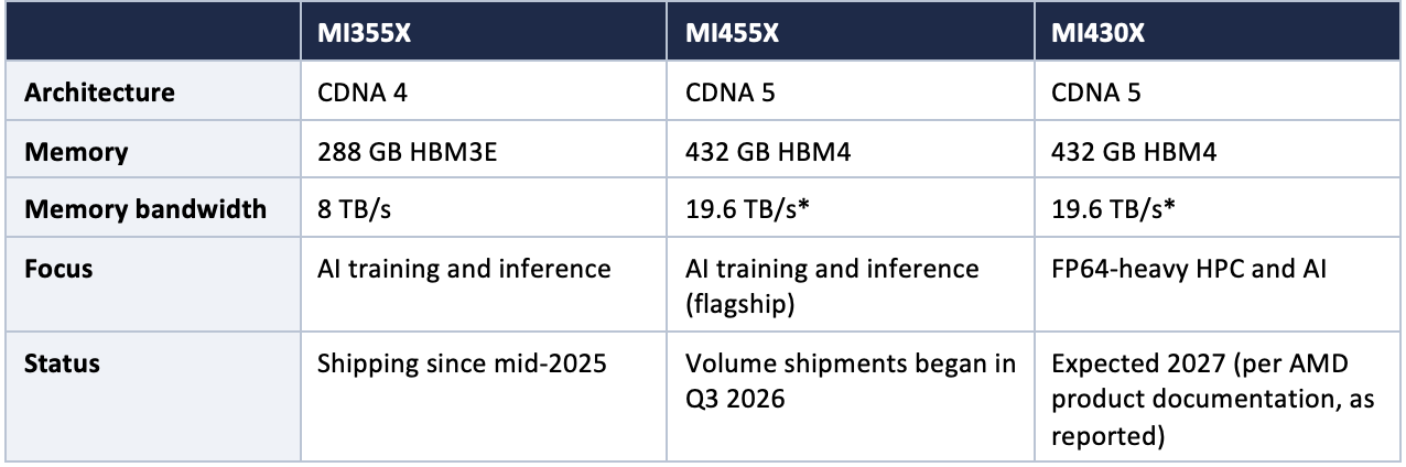
Table 1. Instinct generations. *AMD’s Helios and MI455X product material cites 19.6 TB/s; launch-event coverage cites 23.3 TB/s. This article uses the lower figure (see Caveats).
CPUs: EPYC Venice and Verano
EPYC Venice, launched at AMD’s Advancing AI event in July 2026, is the sixth-generation EPYC: Zen 6 cores on TSMC’s 2nm process, up to 256 cores and 512 threads, a new SP7 socket and PCIe Gen 6. AMD quotes up to 1.6 TB/s of memory bandwidth per socket (16 channels), up from 614 GB/s on its existing parts, and claims more than 70% higher performance and efficiency with over 30% more thread density. Venice is the host CPU in Helios. A second 2nm part, Verano, follows in 2027, tuned for performance per dollar per watt in agentic AI.
Networking: Three Planes
AMD splits networking into three planes, each with its own silicon.
Scale-up (inside the rack). Inside a Helios rack, 72 GPUs form a single scale-up domain with about 260 TB/s of aggregate bandwidth, carried by UALink over Ethernet (UALoE) through switch trays built on Broadcom’s Tomahawk 6. HPE has named its Juniper-based tray for Helios the QFX5252. Native UALink switch silicon was not available in time for the first racks, which is why AMD routes UALink semantics over standard Ethernet. I compared UALink and NVLink in an earlier instalment, and the ESUN article covers the Ethernet scale-up approach.
Scale-out (between racks). Helios uses the Pensando Vulcano 800G AI NIC, which AMD describes as UEC 1.0 compliant. With up to three NICs per GPU, AMD quotes 2.4 Tb/s per GPU and about 43 TB/s per rack. Vulcano follows Pollara 400, which AMD began shipping in 2025 as the first Ultra Ethernet-ready AI NIC; it is programmable through AMD’s P4 engine and stays compatible with RoCE v2. The RoCE v2 and InfiniBand versus Ethernet installments cover the trade-offs underneath.
Front end (storage and network). The Pensando Salina 400 DPU handles software-defined networking, security, storage disaggregation and, according to AMD, KV cache management for AI context, so host CPU cores are not spent on infrastructure tasks.
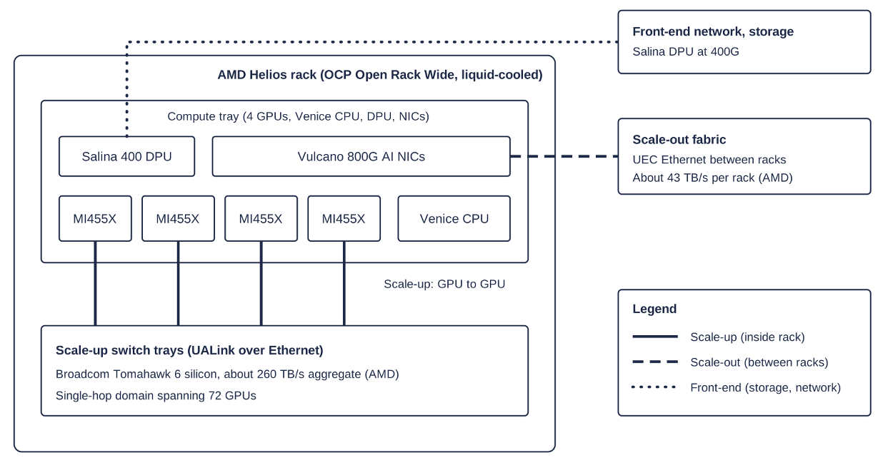
Figure 1. Helios network planes, simplified from AMD and HPE material (not to scale).
The Rack: Helios
Helios packages 72 MI455X GPUs, EPYC Venice CPUs, Pensando networking and ROCm in a double-wide, liquid-cooled rack built to the Open Rack Wide specification that Meta contributed to the Open Compute Project in October 2025. AMD’s stated rack figures are 1.4 exaFLOPS of FP8 and 2.9 exaFLOPS of FP4 compute, 31 TB of HBM4, about 260 TB/s of scale-up bandwidth and about 43 TB/s of scale-out bandwidth.
To build racks, AMD acquired ZT Systems in 2024 for its rack-scale design expertise, then sold the manufacturing arm to Sanmina in a deal that closed in October 2025 while keeping the design and customer-enablement teams. Sanmina is AMD’s preferred new-product-introduction manufacturing partner, and HPE, Dell, Lenovo, Super Micro and other OEM and ODM partners are expected to ship Helios-based systems.
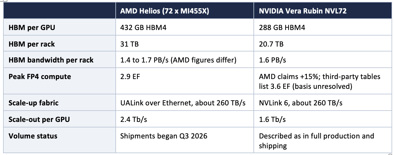
Table 2. Helios versus Vera Rubin NVL72. Helios values are AMD-published or AMD-modeled. NVIDIA values are as cited in third-party coverage and were not checked against NVIDIA’s own datasheets.
Software: ROCm
ROCm 7 arrived with the MI350 launch, and the MI350 series had upstream Linux kernel driver support on day one. In July 2026 AMD declared ROCm 7.14, built on its new TheRock build system, the production release. Under the July 2026 Anthropic agreement, the two companies also plan to use Claude to optimize workloads on Instinct GPUs and accelerate ROCm development. My earlier ROCm article covers the stack itself.
Customers and Ecosystem
The commercial case for the portfolio rests on a handful of very large commitments.
OpenAI (October 2025): a multi-generation agreement for 6 GW of AMD GPUs, with the first 1 GW of MI450-series deployment starting in the second half of 2026. AMD issued OpenAI a warrant for up to 160 million AMD shares that vests as milestones are met.
Meta (February 2026): up to 6 GW across Instinct GPUs, including a custom MI450-based GPU, and EPYC Venice CPUs, with a similar performance-based warrant for up to 160 million shares.
Anthropic (July 2026): up to 2 GW of MI450-series GPUs in Helios racks, with the first gigawatt targeted for the first half of 2027, alongside a potential AMD equity investment of up to $5 billion.
Oracle and Microsoft: Oracle announced plans for Helios deployments and a large MI355X cluster on OCI, and Microsoft plans to run Helios on Azure.
Early results: in its Q3 2026 results, AMD reported record data center revenue of $8.5 billion, up 97% year over year, said MI455X volume shipments began in the quarter, and named Anthropic, Meta, Microsoft, OpenAI and Oracle Cloud Infrastructure as running models and workloads on the first Helios racks.
Honest Caveats
Almost every number is AMD’s. The rack-level figures, the comparison with Vera Rubin NVL72 and the “up to 30% more tokens per dollar” claim are AMD-published or AMD-modeled. Coverage of AMD’s Hot Chips 2026 session noted that independent benchmarks were still scarce. The claim that Vulcano’s scale-out advantage yields 13% faster LLM training comes from modeling an 8,000-GPU system, not from measured deployments.
Source conflicts I could not resolve. MI455X memory bandwidth appears as 19.6 TB/s in AMD’s Helios and MI455X product material and as 23.3 TB/s in launch-event coverage, and the rack totals follow (1.4 versus 1.7 PB/s). I use 19.6 TB/s, the more conservative figure. The FP4 comparison is also unclear: AMD claims 15% more peak FP4 than Vera Rubin NVL72, yet third-party tables list 2.9 EF for Helios against 3.6 EF for NVIDIA’s rack. The two probably rest on different bases, but I could not reconcile them from public material. Descriptions of the scale-up switch hardware also differ: AMD’s product page refers to four scale-up cartridges, while other coverage describes six switch trays.
“Open” scale-up is not native UALink. The first racks tunnel UALink over Ethernet because native UALink switch silicon was not ready. The Register has reported that tunnelling will not come close to UALink’s 100 to 150 ns latency target. An open specification also does not mean interchangeable parts: today’s validated path is a specific combination of AMD GPUs, a Broadcom-based HPE Juniper switch tray and AMD NICs. That is a different kind of lock-in from NVLink, but it is still a tightly coupled stack.
Host-to-GPU bandwidth trails. StorageReview’s comparison lists a 256 GB/s Infinity Fabric link between each MI455X and its Venice host, against 1.8 TB/s of NVLink-C2C that one NVIDIA Vera CPU shares across two Rubin GPUs. That gap may matter for CPU-resident KV caches and offload.
Financial structure and concentration. The OpenAI and Meta agreements each carry warrants for up to 160 million AMD shares, and AMD recorded a $1.1 billion non-cash charge in Q3 related to customer warrants, which it expects to grow as customers progress. For Anthropic, AMD has committed to a possible equity investment alongside the hardware order. The announced commitments now total roughly 14 GW and rest on a rack platform that only began volume shipments in the third quarter. Customers who are also investors or shareholders make demand harder to read than ordinary purchase orders.
Execution risk is not behind AMD yet. Earlier in 2026, reports (SemiAnalysis among them) pointed to 2nm integration challenges and a possible MI455X delay; AMD denied it and later reported volume shipments. By AMD’s own description the ramp is still early. Each rack needs about 31 TB of HBM4, so memory supply is a shared constraint, and a liquid-cooled 72-GPU rack likely demands facility readiness that many data centers lack. The MI430X is not expected until 2027.
Software is maturing, not mature. ROCm 7.14 arrived with a version-numbering discontinuity that AMD’s own release notes acknowledge, and the 7.14.1 update in September restored RCCL collective performance on InfiniBand. That is normal for a fast-moving stack, but the depth of the CUDA ecosystem is still the benchmark.
Pricing is opaque, and roadmap items are targets. AMD has not published Helios pricing. Futurum Group, cited by CNBC, estimated $5 to 5.5 million per rack against $3.5 to 4 million for NVIDIA’s next platform; these are estimates. MI500, Verano and the 2027 rack are forward-looking statements, as are AMD’s 2030 targets from its November 2025 analyst day.
Outlook
AMD says Helios deployments should increase substantially in the fourth quarter as HPE, Dell, Lenovo, Super Micro and other partners begin shipping systems. Its next rack, combining EPYC Verano, Instinct MI500 and Vulcano networking, is slated for 2027, and management has said it expects revenue growth of more than 80% in 2027 based on current visibility. This should be treated as a company expectation, not a settled forecast.
What deserves to be watched: independent inference results on MI455X and Helios, the arrival of native UALink switch silicon, HBM4 supply, and how the first gigawatt-scale deployments perform in uptime and cost per token, not just in peak specifications.
I may have missed deployments or data points. If you have measured Helios or MI455X yourself, or spotted a figure I should correct, please comment and I will add it to this article.
References
https://www.amd.com/en/products/rackscale-solutions/helios.html
https://www.amd.com/content/dam/amd/en/documents/solutions/ai/amd-helios-bro.pdf
https://www.sec.gov/Archives/edgar/data/0000002488/000000248826000188/amdq32026earningsslidesf.htm
https://www.fool.com/earnings/call-transcripts/2026/11/04/amd-amd-q3-2026-earnings-call-transcript/
https://www.benzinga.com/news/26/11/62849372/advanced-micro-devices-q3-2026-earnings-call-transcript
https://hothardware.com/news/amd-partners-anthropic-2-gigawatt-mi450-chip-deal
https://www.artificialintelligence-news.com/news/amd-anthropic-ai-infrastructure-deal/
https://hothardware.com/news/amd-inks-meta-ai-deal-deploy-6-gigawatts-gpus-data-centers
https://www.amd.com/en/blogs/2025/amd-cements-data-center-leadership-at-financial-analyst.html
https://www.eenewseurope.com/en/amd-maps-out-strategy-for-leadership-in-future-compute-and-ai
https://amd.com/en/blogs/2025/amd-helios-ai-rack-built-on-metas-2025-ocp-design.html
https://www.amd.com/en/blogs/2025/powering-next-gen-ai-infrastructure--a-new-era-of.html
https://www.amd.com/zh-cn/blogs/2026/ai-networking-built-for-scale.html
https://www.fierce-network.com/cloud/amds-helios-bets-ai-networking-open-ethernet
https://rocm.docs.amd.com/en/docs-7.14.1/about/release-notes.html
https://www.servethehome.com/amd-helios-architecture-deep-dive-amd-broadcom-hardware-combined/4/
https://www.theregister.com/2025/07/15/broadcom_ethernet_scale_up/
https://www.theregister.com/2025/12/02/hpe_amd_helios_racks/
https://www.jonpeddie.com/news/amd-instinct-455x-targets-nvidias-rubin-directly/
https://ai2.work/blog/amd-helios-at-hot-chips-2-9-exaflops-and-31tb-hbm4-in-one-rack
https://www.sdxcentral.com/control-plane/5-things-we-learned-from-amds-advancing-ai-2026/
https://www.techspot.com/news/112492-amd-256-core-epyc-venice-enters-production-tsmc.html
https://hpcwire.com/2026/08/03/amds-fp64-boost-with-mi430x-is-even-bigger-than-expected
https://itbrief.co.uk/story/amd-unveils-instinct-mi430x-gpu-to-power-next-gen-supercomputers
https://tech-insider.org/ca/amd-mi400-hbm4-nvidia-rubin-b300-2026/
https://thenextweb.com/news/amd-advancing-ai-helios-mi455-cerebras-nvidia
https://convergedigest.com/amd-finalizes-sale-of-zt-systems-manufacturing-operations-to-sanmina/
https://tech.yahoo.com/computing/articles/amd-helios-ai-rack-sparks-192300885.html
